|
|
|
|
|
|
Every now and then I need a preamplifier for measurements and other purposes. For quite a long time I used a provisional one, but together with the Universal Filter and the Weighting Filter Set I decided to realize a more professional one.
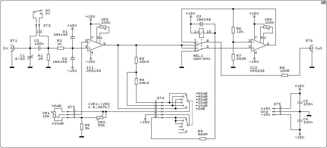
As my provisional one had an adjustable gain of up to 40 dB and this maximum gain usually was used I thought it might be a good idea to provide a gain of up to 60 dB. The big advantage of this factor of 1000 is that all readings on meters or oscilloscopes in Volt easily can be interpreted as Millivolt, which makes it quite simple and safe to use.
The gain is adjustable in steps of 10 dB from 0 dB up to 50 dB and by a vernier potentiometer another 10 dB, so there are 60 dB over all.
| dB vs. Voltage Gain | |||||||
| dB | 0 | 10 | 20 | 30 | 40 | 50 | 60 |
| Gain | 1 | 3.162 | 10 | 31.62 | 100 | 316.2 | 1000 |
The first stage has an adjustable gain of 0 - 30 dB, the second stage has a fixed gain of 30 dB and can be activated by a relay. Because within the audible band (i. e. up to 20 kHz) no noticable gain loss shall be observable two stages for a total gain of 60 dB are minimum. The first stage uses an OPA134 with a gain-bandwidth of 8 MHz so the cutoff frequency at 30 dB gain is a reasonable 270 kHz approx.. Anyway - next time I'll rather head for three stages. As the op-amp of the second stage always has a gain of 30 dB an uncompensated op-amp with a higher open-loop gain may be used. I selected an OPA 228 with a GBW of 33 MHz, so this stage should have a bandwidth of 1 MHz. For better noise performance I did not use an input divider network as they are common in multimeters or oscilloscopes.
The high input impedance of 1 MOhm allows to optionally connect a 10:1 oscilloscope probe but requires an FET-type op-amp. With the adjustable C1 the input capacitance can be adjusted equal to that of the oscilloscope where the probe pinched off. (In my sample the wiring capacitance is so high that even a 6 pF parallel capacitor is slightly too much.) When such a probe is to be used the input wiring must be shielded. At a gain of 1000 even little capacitive feedback from the output makes the gain rise at higher frequencies - up to some dB. This should be avoided.
Using a relay to loop in the second stage is much cheaper and easier to wire than with an adequate rotary switch (i. e. 3P6T instead of 2P6T). The relay used here has a 24 V coil of 2.4 kOhm approx, so a series resistor of about 600 Ohm is needed for 30 V operation.
Assuming R5 = 3 kOhm requires a potentiometer of (3.162 - 1) * 3 kOhm = 6.487 kOhm. This must be adjusted by VR2. The other resistors ideally would be: R3 = 20.513 kOhm and R4 = 64.868 kOhm. The next values from the E96-series are 20.5 kOhm and 64.9 kOhm deviating -0.06% and -0.05% only from the ideal values. For the 2nd stage with R6 : R7 = 12 kOhm : 392 Ohm the gain becomes 31.61 (= -0.03% error, the best 30 dB match you get using E96) or, using E24 only, 11 kOhm : 360 Ohm results in a gain of 31.55 (= -0.2% error).
The input referred noise of a high gain preamplifier should be most important. In this circuit it is determined by resistors R2 to R5, VR1 parallel to VR2 and by the input op-amp IC1. It is very much depending on the actual gain setting. It is least at gain = 1, when only R2 (1 KOhm: 4 nV/sqr(Hz)) and IC1 (OPA134: 8 nV/sqr(Hz)) contribute to the noise, resulting in 9 nV/sqr(Hz) or 1.3 uV measured bandwidth limited up to 20 kHz. It is worst when the output impedance of the feed-back network is highest. For more noise values see table below. I find them to be quite high - I'm regaled by op-amps available with less than 1 nV/sqr(Hz) (but not as FET-types). So what can we do?
First I propose to reduce the feedback network impedance (R3 to R5, VR1 and VR2) by a factor of 10. This creates quite a big load for IC1, and I fear distortion, but you can't get it all. Further I'd reduce R2 to 470 Ohm. With these measures the resistor depending worst case noise becomes 4.7 nV/sqr(Hz), much less than the OPA134 creates. Furthermore, by using an OPA627, an extremely expensive, lowest noise audio FET op-amp (4.5 nV/sqr(Hz)) the worst case input referred noise is reduced to 6.5 nV/sqr(Hz) or 0.92 uV (always measured up to 20 kHz).
The other way around, with the common TL071 (18 nV/sqr(Hz)) and the higher resistor values a worst case noise of 22 nV/sqr(Hz) or 3.1 uV (up to 20 kHz) will be achieved.
|
|
Noise density (per sqr(Hz)) | Noise measured from 20 Hz to 20 kHz | |||||
| Op-Amp | RX | Best Case | Max. Gain | Worst Case | Best Case | Max. Gain | Worst Case |
| TL071 (18 nV/sqr(Hz)) |
|
18.5 nV | 19.7 nV | 22 nV | 2.6 uV | 2.8 uV | 3.1 uV |
|
|
9.0 nV | 11.3 nV | 15 nV | 1.3 uV | 1.6 uV | 2.1 uV | |
|
|
8.5 nV | 8.7 nV | 9.3 nV | 1.2 uV | 1.25 uV | 1.3 uV | |
| OPA627 (4.5 nV/sqr(Hz)) | 5.3 nV | 5.7 nV | 6.5 nV | 0.75 uV | 0.81 uV | 0.92 uV | |
Best Case: Stage 1 gain = 1, i. e. output of IC1
is directly conected to its negative input
Max. Gain: Stage 1 gain = 20 dB, i. e. VR1
is turned towards R5, low feed-back network output
impedance
Worst case: Stage 1 gain = 20 dB with VR1
turned towards R4, highest feed-back network output
impedance
RX: x 1: All values
as in the circuit diagram above, x 0.1: R3,
R4, R5, VR1
and VR2 = 1/10 of the values
above, R2 = 470 Ohm
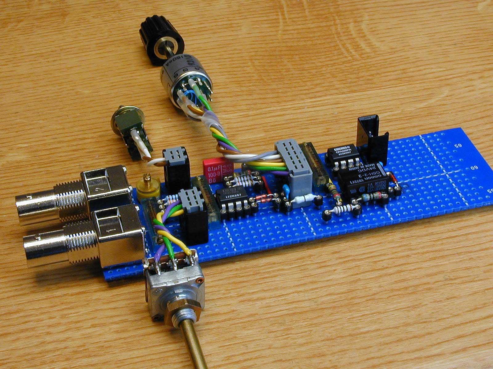
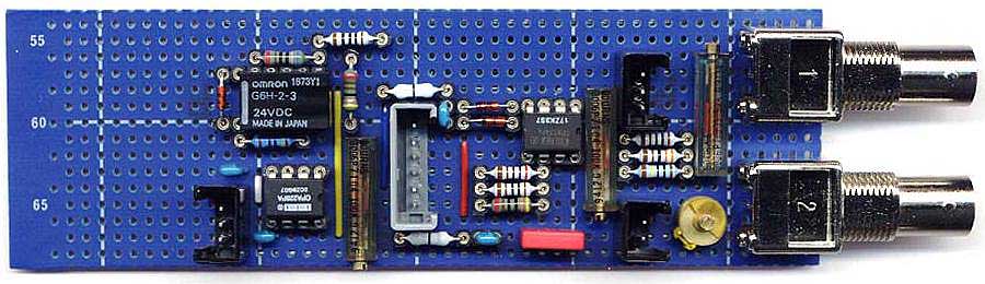
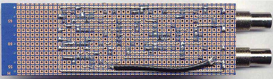
My favourite way is to use a special kind of square pad board (Vero) and to spend a lot of time designing the layout and its implementation because I very much enjoy the aesthetic aspects of electronics. Perhaps somebody else feels like me.
The input section is not shielded here, which I really do regret. Next time I'll do it better, I promise.
| Last update: October 13th, 2015 | Questions? Suggestions? Email Me! | Uwe Beis |