| |
|
Design of the LNPA60dB
(![]() German Version: Entwicklung des LNPA60dB)
German Version: Entwicklung des LNPA60dB)
Development experience and detailed measurement results
| |
|
Design of the LNPA60dB
(![]() German Version: Entwicklung des LNPA60dB)
German Version: Entwicklung des LNPA60dB)
Development experience and detailed measurement results
This article is an extension to the main article Ultra Low Noise FET Pre-Amplifier. It gives a small insight into the development of the LNPA60dB (Low Noise Pre-Amplifier with up to 60 dB Gain) and also contains further measured values.
I had already developed an especially low-noise preamplifier with FET operational amplifiers connected in parallel, the LNPA40dB. Because of the operational amplifiers it can be used for DC signals and because of the moderate current consumption also for battery operation. The achieved 2.2 nV/√Hz are comparatively good, but with parallel connected J-FETs a pure AC preamplifier can be made with much less noise. With 6 low-noise JFETs in the input, I achieved 0.41 nV/√Hz. This is roughly equivalent to the thermal noise of a 10 Ω resistor.
It was not my first attempt to develop such a preamplifier using this principle, but it was the first successful attempt.
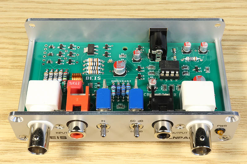
 First I designed the preamplifier as an experimental setup. Nearly all resistors can be mounted either leaded in the form 0207 or as SMD in the form 0805. In the experimental setup I have provided them with sockets into which the resistors can be plugged for experimental purposes. On the board there are up to 6 JFETs equipped, of which there are only 2 populated in the sample, but on a plug-in module there are another 4, because of course it is interesting how the differences are with different numbers of JFETs.
The gain is switchable between 40 and 60 dB. It is technically not useful and even hardly possible to realize smaller gains. This has the following reason:
All resistors in the input contribute with their thermal (and possibly also current induced) noise to the input noise of the amplifier. Not only the series resistors (protective resistors) in the input or the output impedance of the source. Also the output impedance of the negative feedback matters: To set a certain gain, a voltage divider is needed which divides the output voltage of the amplifier to the negative feedback in inverse ratio to the gain. So, for example, at 60 dB gain in the ratio 1000 : 1. If I want to achieve an input noise that corresponds, for example, to the thermal noise of a 10 Ω resistor, the output impedance of this voltage divider must be far below 10 Ω, because it should have a minimum influence on the total noise.
In the LNPA the output resistors of the voltage divider across which the source current of the 6 JFETs flows, consist of 4 10 Ω resistors connected in parallel. The output impedance of the voltage divider is therefore 2.5 Ω. For 60 dB gain the series resistance must be 999 times, i.e. approx. 2.5 kΩ, for 40 dB still approx. 250 Ω. These 250 Ω load the output driver of the preamplifier not insignificantly, but tolerably. If one wanted to set 20 dB gain, the load for the output driver would be 25 Ω. This would require a special effort.
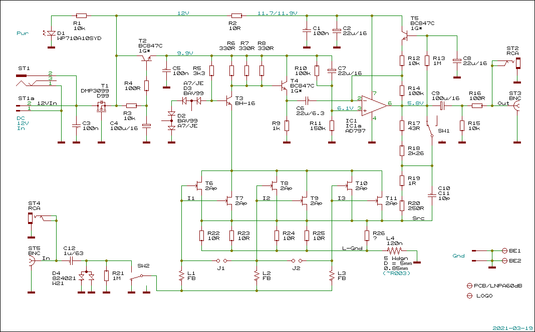
The JFETs operate at 0 V bias voltage so that their drain current is maximal, because in doing so they achieve minimum noise of about 1 nV/√Hz. To keep the bandwidth high and the Miller capacitance low, the drain current goes through a cascode circuit with NPN transistor to a working resistor. This is visible in the picture and consists of 3 330 Ω resistors connected in parallel (the 4th resistor has 3.3 kΩ and does not belong). This preamplifier has a relatively low gain of only about 14 (= 12 dB), so the following opamp must also be very low noise. An AD797 with about 1 nV/√Hz resulted in another significant gain compared to the originally planned OPA228 with about 3 nV/√Hz. However, this opamp is one of the most expensive low-power ones I know of. Alternatively, an LT1128 should give the same results for about the same price.
To ensure that the gain is precisely 40 or 60 dB, 0.1% resistors are used in the negative feedback. This initially only achieves that the difference between 40 and 60 dB is precisely correct. With the 4 10 Ω resistors 0.1% versions would not help. That's why there (instead of a trimmer) a trimming resistor is provided parallel to the 2.5 Ω, which amounts to several 100 Ω depending on the specimen.
 After the first build (Rev.0) the second one (Rev.1) is now ready. New findings have arisen and the circuit has been slightly expanded and optimized. From this revision on a different housing is intended for the LNPA60dB.
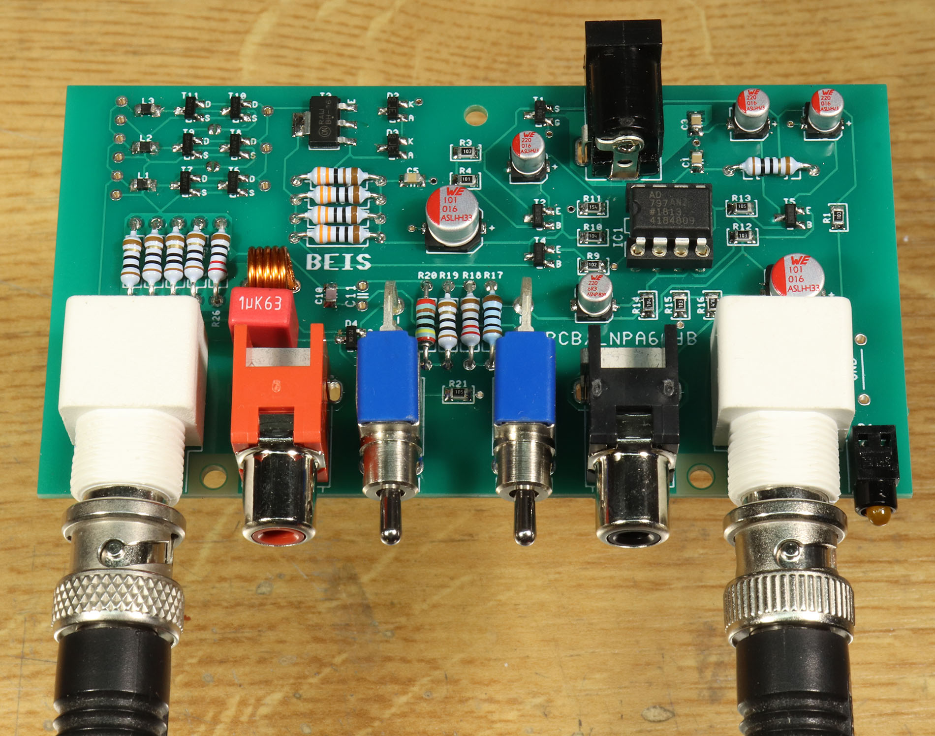
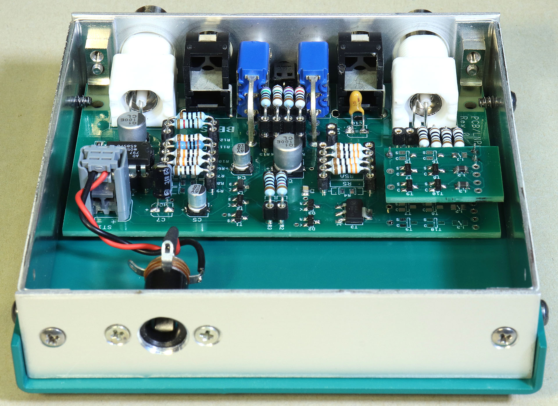
The applied changes were adopted in the next PCB revision (Rev.3, left) (Rev.2 was discarded because I had to correct something shortly after ordering the Rev.2 boards). This also included more SMDs instead of leaded resistors. So it was ready for a first small series. There were new measurements, some more experiences to collect and the final dimensioning for exact amplifications to fix. Also front and back panels for the already existing cases could now be ordered.
Measured with 6 JFETs at 60 dB gain. The noise density could be determined in two ways from the output signal: 1. converted via my ADC AD24QS and the noise spectra determined from it, and 2. also in a purely analog way with a following 60 dB amplifier, a weighting filter 20 Hz - 20 kHz and a true RMS voltmeter. Both results were practically identical.
Further measured values can be found in the main article.
10 noise spectra I show here. They are created with my AD24QS as ADC. Like many other typical delta-sigma audio ADCs, this one shows a rapid increase of intrinsic noise above 50 kHz because of the so-called noise shaping.

- Click graphic for enlarged view -
The following spectral lines are important:
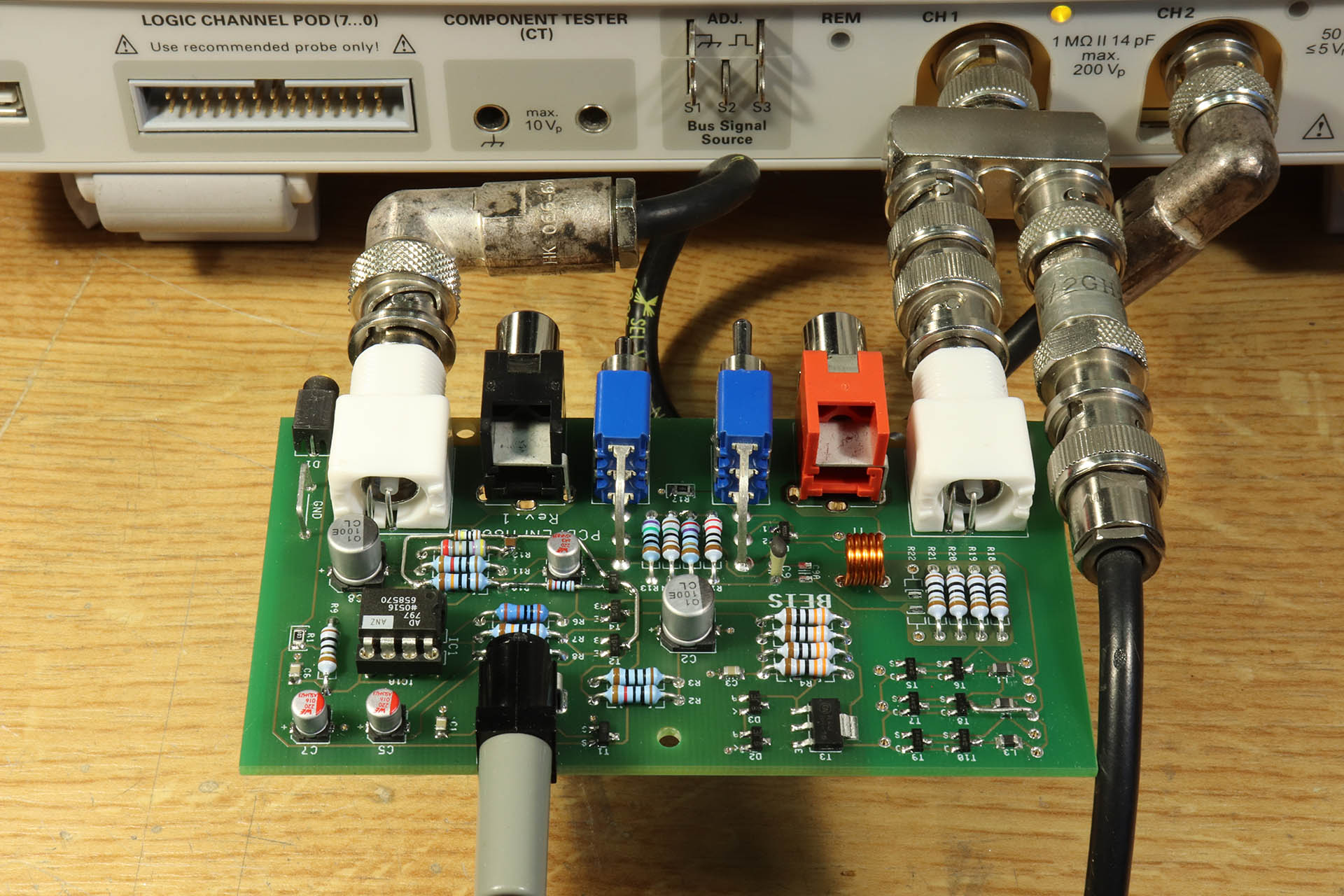
Unfortunately, I do not have a special device for determining the amplitude responses. So I used my oscilloscope with FFT and two function generators. One function generator can generate up to 50 MHz, the second one generates for the first one a very slow frequency modulation ramp for a sweep from 0 to 10 MHz. Such a sweep takes about 3 hours to get with the oscilloscope's envelope display a reasonably clean frequency responses like this.
Unfortunately, the scaling of only the Y-axis, but not the X-axis, is logarithmic as usual. The numerical output of the measured values is also not possible because of the envelope display, otherwise I would have liked to display it double logarithmic.
Furthermore, the range from 0 to 10 MHz is divided into 12 divisions. This is impractical and results in 833 kHz per division.
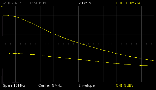
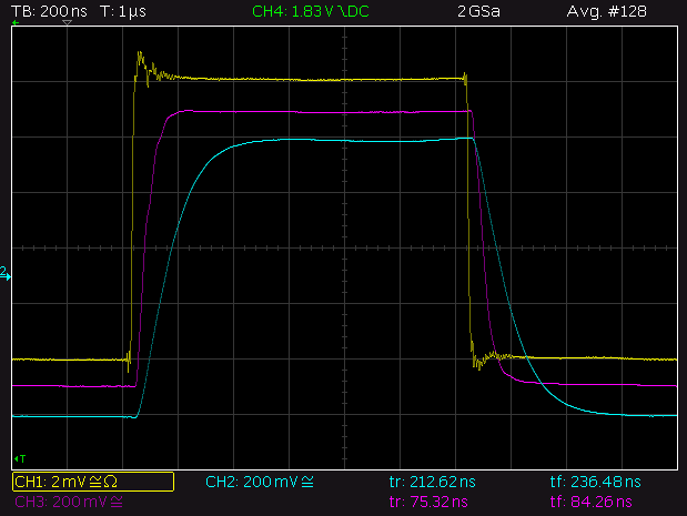
To determine the step response, the generator provides a square wave signal with about 7 ns rise time. The rise time at the output of the LNPA60dB is limited by the finite slew rate of the AD797. Therefore, in principle, for both, the determination of the amplitude response and for that of the slew rate, the output voltage must be relatively small. At more than 500 mV within 70 ns this limit is approximately reached.
In principle, even lower input noise can of course be achieved by further parallel connection. However, this is not the case in this experimental setup. Any number of JFETs could be added, but without further reduction of the negative feedback impedance this would not be very effective. Smaller resistance values in the negative feedback would again require a larger output power of the op-amp, but it should not be loaded much higher than it already is now, at least at 40 dB gain. If only 60 dB gain is provided, it should be possible.
However, it could also work to simply connect e.g. 4 of these preamplifiers with their inputs and outputs in parallel, which should then halve the input noise. 0.2 nV/√Hz would really be an extraordinary value.
| Last update: April 7th, 2021 | Questions? Suggestions? Email Me! | Uwe Beis |