The ADDA2-QC Project
For a long time it seemed that I would no longer be able to offer the fully developed successors to the AD24QS and DA24QS.
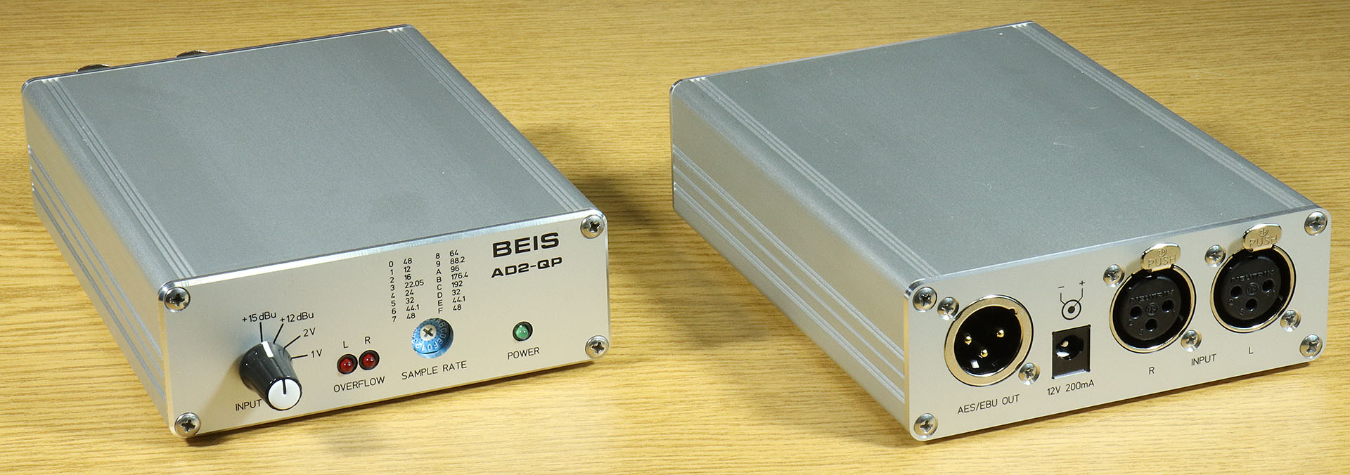
But now (as of June 2025) at least the ADC kit is available, either in the planned consumer version (AD2-QC) or in a version for professional use (AD2-QP)
( German Version: Das Projekt ADDA2-QC)
Inhalt
Preface
Overview
Details
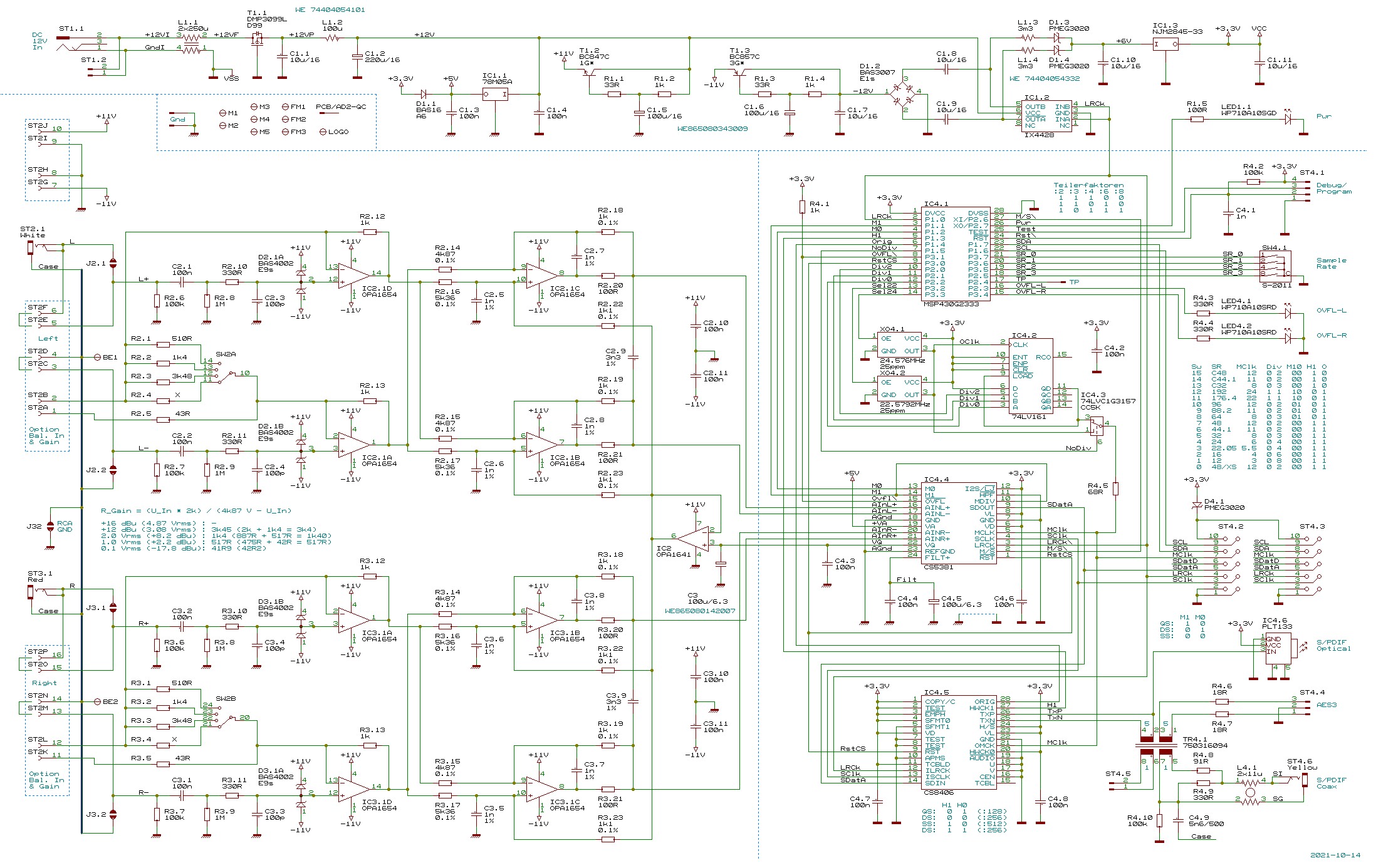
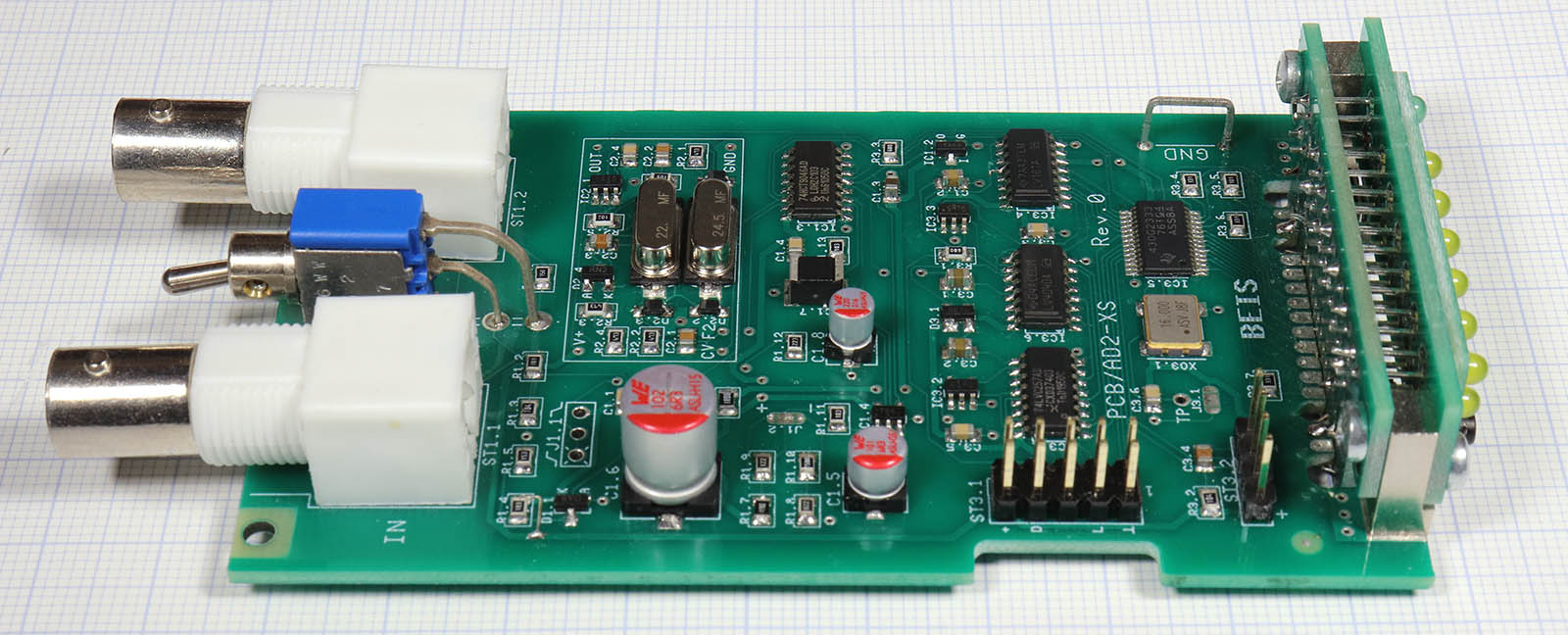
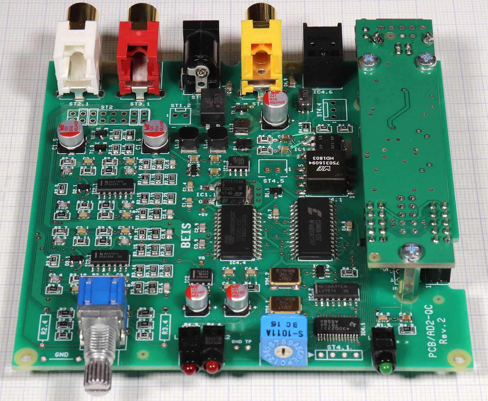
The ADC AD2-QC
The DAC DA2-QC
Word Clock Synchronization with the AD2-XS
The USB interface UIC22
Enclosures
Epilogue
Preface
Preface to the preface (September 2025):
The following text was written over 3 years ago. Little has changed for a long time, but the semiconductor crisis is long gone. The new grief was that kits now also have to comply with WEEE regulations. I wouldn't have been prepared to shoulder the burden. That's not exactly motivating either.
But then I received an inquiry about the delivery of a “non-negligible” number of ADCs, albeit for professional use, i.e. in a professional version. A good start to pick up the thread again. The WEEE problem was solved by the fact that the distribution could be handled by the company of a good friend with whom I had already realized other projects, because the WEEE regulations are fulfilled there. The only remaining hurdle was an IC that had been discontinued in the intended housing and was no longer available. However, as it was still available in another housing, this hurdle could also be overcome by changing the layout.
So there are now two different kits:
- The professional version AD2-QP, which is equipped exclusively with XLR inputs and outputs and includes a housing, and
- The consumer version AD2-QC, which is equipped with RCA sockets for analog audio and S/PDIF and an optical digital output (TOSLINK) and which can optionally include a USB interface.
In terms of technical data and functions, the two variants do not differ. What has changed is that instead of the former input sensitivity of +16 dBu, +15 dBu is now provided because this is an ARD (German public radio) standard.
When and where will kits and ready-made devices be available?
It is planned that kits and ready-made devices will be offered by Heroms GmbH. The USB interface UIC22IC is also expected to be available at the ADC. This is a further development of the UIC22 and now includes galvanic isolation of the USB part from the audio ground and a USB-C connection. Further assemblies, in particular the DA2-QC, are not currently planned.
Information on the kits can be found in the articles AD2-QC and AD2-QP. Some more details about both ADCs can be found below.
The original preface, now partially outdated:
This is the state of affairs in January 2022. My previous ADC and DAC kits, the AD24QS and DA24QS, are partly already sold out, can hardly be reproduced and should not be reproduced at all. Not least because some components were already 15 years ago, when I started with the kits, no longer the most actual ones and are now long discontinued. Of course I also wanted to realize new ideas, but on the other hand I don't want to forget the old ideas and experiences.
So in the last months I have developed a new generation, which is based on the previous experiences and standards, but in addition offers some new and often desired possibilities. At least the ADC should have been available around since the end of 2021 - that was the plan.
But before that came the semiconductor crisis. Nothing works anymore. At least almost nothing. But it's not enough if I can get 98% of the parts, sometimes with great effort, but 2% can't be found anywhere or can't be replaced by others. In addition, there is the experience that components, which are still in stock according to availability, are no longer available shortly afterwards.
Example: I wanted to order 30 transformers for the DA2USB, but they were nowhere available, not even in China. Only at a well-known and reputable distributor from the USA, according to their website in February 278 pieces should be available. Better than nothing - so I ordered there. With the order confirmation there came suddenly a funny surprise: Only 1 transformer instead of the 30 ordered and the allegedly 278 available should come. The rest should be delivered in June. Such an experience shapes.
I can only hope that the new project will be completed this year (2022). But the way the situation is developing, I don't have much hope.
If you are interested in the progress of the project, or when something will be available, you can send me an email. I've set aside a mailing list for that purpose. And last but not least, because of my notorious curiosity, what would be of interest and what part of the world are you from? Here are the hints for e-mails.
State of March 2022: The semiconductor situation seems to get rather worse. I don't have any useful statistics, but I estimate that by now half of all semiconductors, at least the ones I was looking for, are listed with delivery times of more than one year.
I have revised the USB interface UIC22: There will now be galvanic isolation between the audio and PC grounds. This is a very important feature - how could I have missed it before? Fortunately it is not too late. But I can't build a prototype, because the required digital isolators (2 slightly different ones) are - of course - sold out. Both the desired ones, as well as similar, compatible ones.
Overview
At least I'd like to present here what I've developed and what should be available someday. First the similarities and differences in keywords:
The (planned) kits:
- AD2-QC: The ADC, 24 bit, up to 192 kHz
- DA2-QC: The DAC, 24 bit, up to 192 kHz
- UIC22: USB/I2S converter (USB Audio Class 2) that can be plugged onto the ADC, with stereo inputs and outputs
- AD2-XS: Add-on module with high-quality VCXO for eXternal synchronization of the ADC via word clock
Same or almost the same:
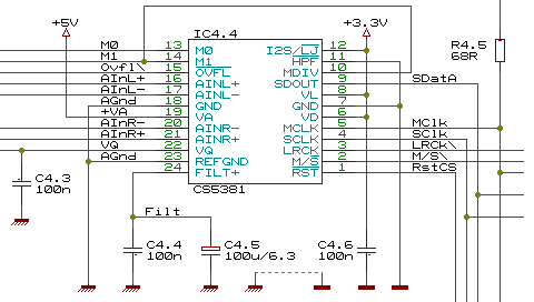
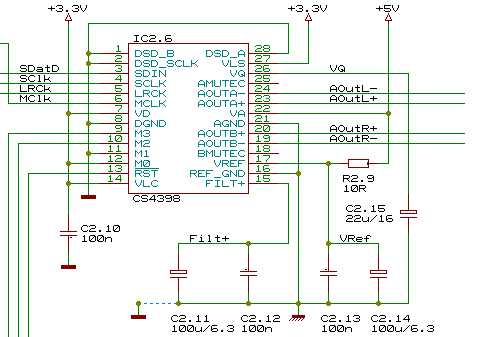
- The same chipsets as before (ADC: CS5381 and CS8406, DAC: CS8496 and CS4398)
- The same connectors as before (RCA inputs and outputs as well as S/PDIF and Toslink)
- ADC: 12 (instead of 10) sample rates: 12, 16, 22.05, 24, 32, 44.1, 48, 64, 88.2, 96, 176.4 and 196 kHz
- ADC: Consumer format 32, 44.1 and 48 kHz, but now without copy protection
- Expandable for balanced inputs/outputs and AES3 connections
- 12 V power supply
- Approximately the same dimensions (~100 x 100 mm)
- Provided: Enclosures (continuous casting) with front panels available for standard versions
New or modified:
- Kits prefabricated in SMD technology. Only connectors, switches and indicators have to be completed
- DAC: There is an I2S input to connect a UIC22
- ADC: 4 different gain values switchable, one of them programmable by post-assembly resistors
- One ADC (master) can synchronize other ADCs (slaves) via an I2S input/output
- With the AD2-XS one or more ADCs can be synchronized with word clock
- The USB module UIC22 can be plugged directly onto the ADC
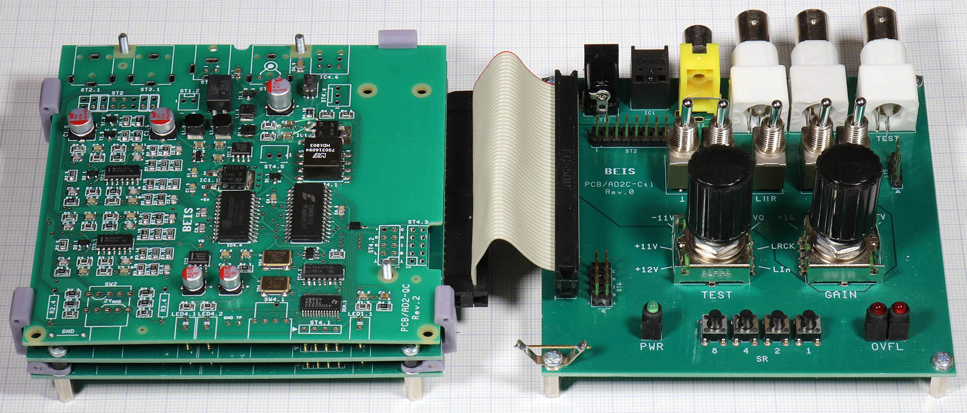
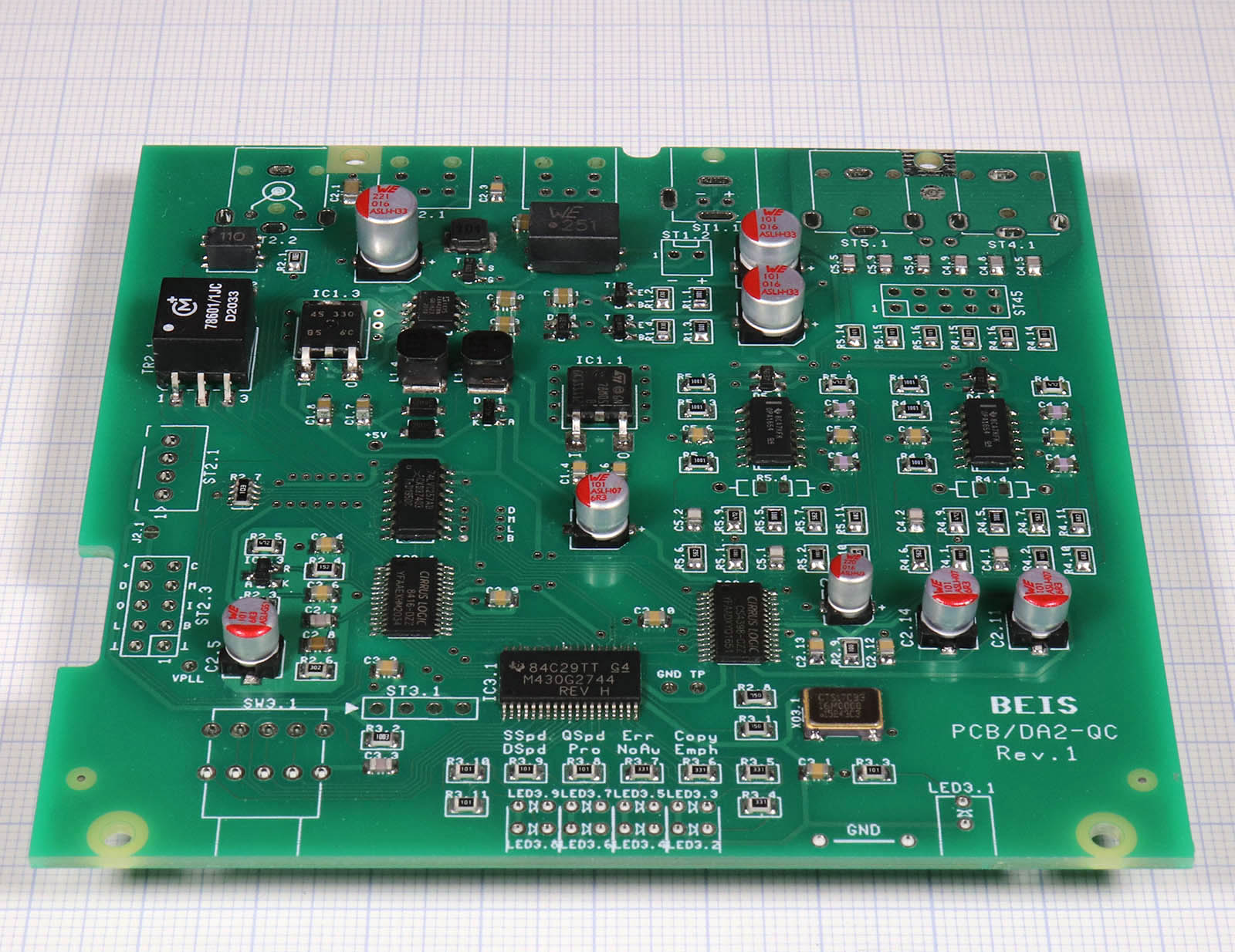
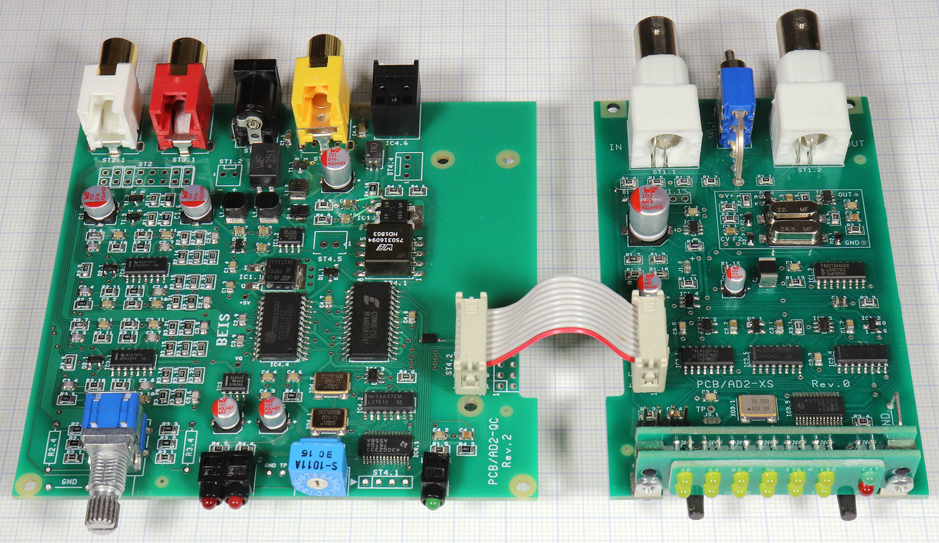
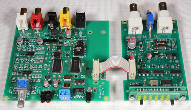
The SMD-equipped modules are tested on special test adapters before delivery:
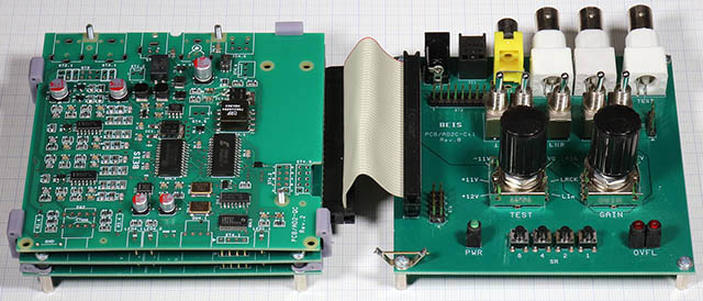
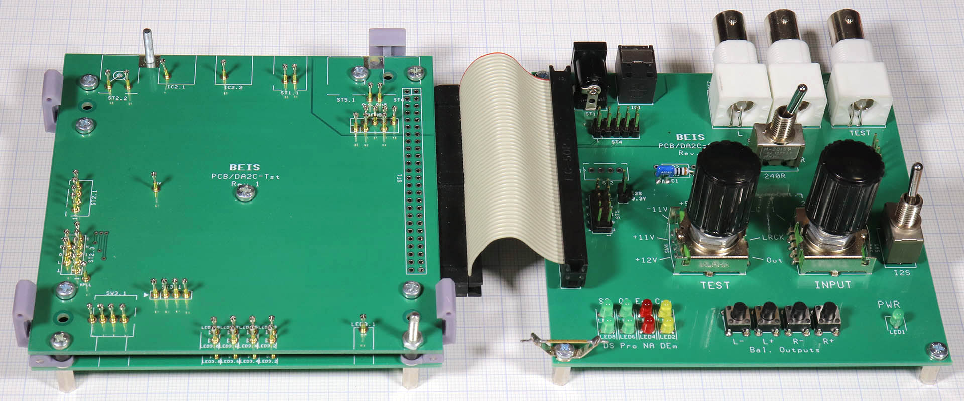
Here the AD2-QC is clamped on its test adapter. For the DA2-QC there is a very similar test adapter:
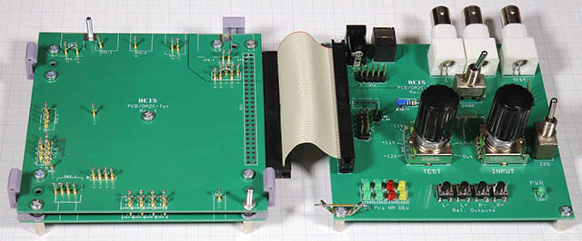
Here the DA2-QC is not clamped.
Details
Such a development usually requires several revisions of the lab samples or prototypes. In the process, experience is gained, i.e. what has not proved successful is improved or new ideas are incorporated, etc.. Example: The ADC has already been revised 3 times (so far). I don't have the latest revisions of the assemblies yet, the photos here are from the (so far) most recent revisions. I will add newer photos later.
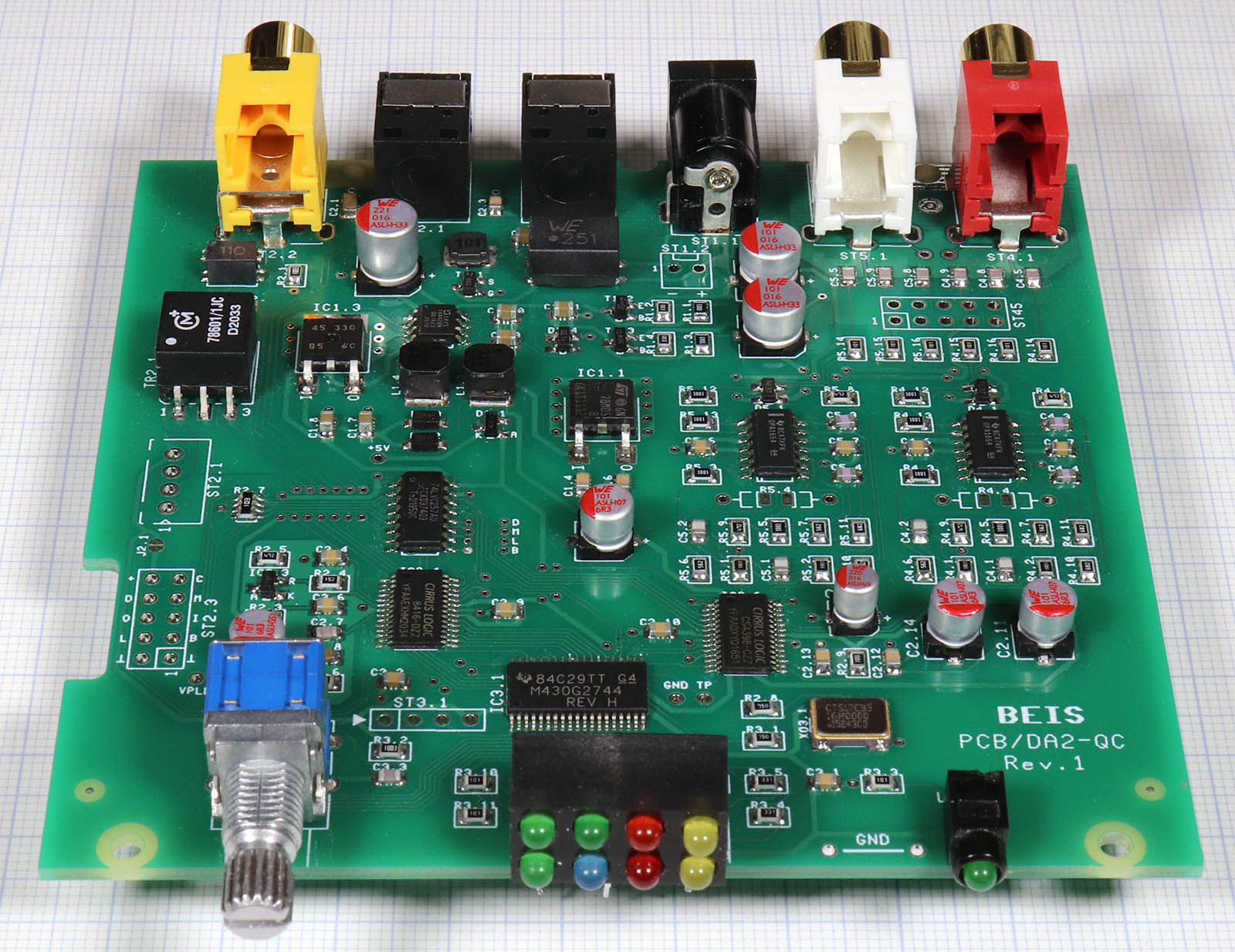
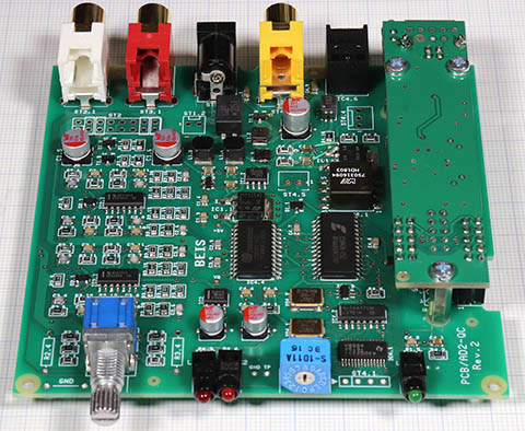
The ADC AD2-QC
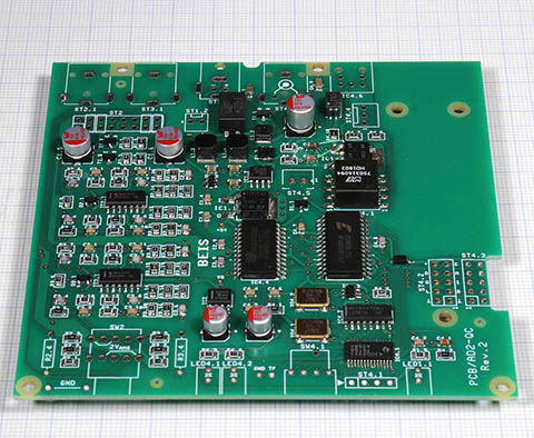
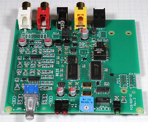
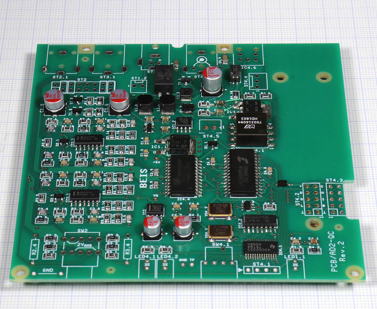
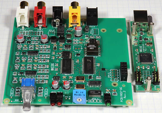
Pictures: View of the SMD-only ADC and the one completed with THT components, without additional connections.
 The circuit does not contain any unusual tricks. The analog part is similar to the AD24QS. Low noise audio class FET operational amplifiers are now used.
External balanced analog inputs, usually XLR jacks, can be connected together with a toggle switch to switch between the on-board RCA jacks and the external inputs, and a potentiometer or switch to adjust the gain via a header. This is like the AD24QS. A preamp can also be looped in there. There could be a phono preamp, for example.
The gain or sensitivity of the ADC can be switched with a 4-position switch to different values, which are common in the consumer or professional range. For 100% FS are provided:
- +16 dBu (~4.9 Vrms)
- +12 dBu (~3.1 Vrms)
- 2 Vrms (~+8.2 dBu)
- 1 Vrms (~+2.2 dBu)
With additional THT resistors, which are inserted into the spaces kept free for this purpose, 0.1 Vrms to +16 dBu can be set.
The generation of the negative and about half of the operating voltage is done in a somewhat unusual way with the frequency of the sampling rate, so that there can be no more even minimal spikes in the spectrum outside the audible range. This sounds simple and looks like it, but in development it caused me no small amount of headaches. The goal was also to reduce the power consumption again considerably compared to the predecessor. The operating current is always less than 110 mA for the current prototype.
The operating voltages of the preamplifier are, as with the predecessor, filtered again extra, so that also power supplies with larger ripple can cause no big disaster.
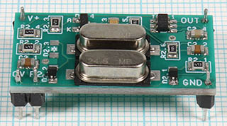
The clock generation is done by two separate crystal oscillators, a prescaler and otherwise the ADC IC. 2 10-pin I2S connectors can be input or output. As pin headers they are available for the connection to one or more further ADCs for external synchronization or as (mirrored) socket header for the plug-on USB interface. Especially if several ADCs are to be clocked by the I2S signal of a master ADC, an I2S buffer might be required as line driver for the I2S output of the master. The I2S-Buf shown on the right is simply inserted into the I2S line with 2 10-pin headers.
A µC is used for the control, which also monitors whether the ADC should work autonomously or should be synchronized by another ADC or the AD2-XS.
The digital outputs are transformer-coupled - as it should be if you want to do it properly. An AES3 output can be connected directly, also for it a transformer output is already provided.
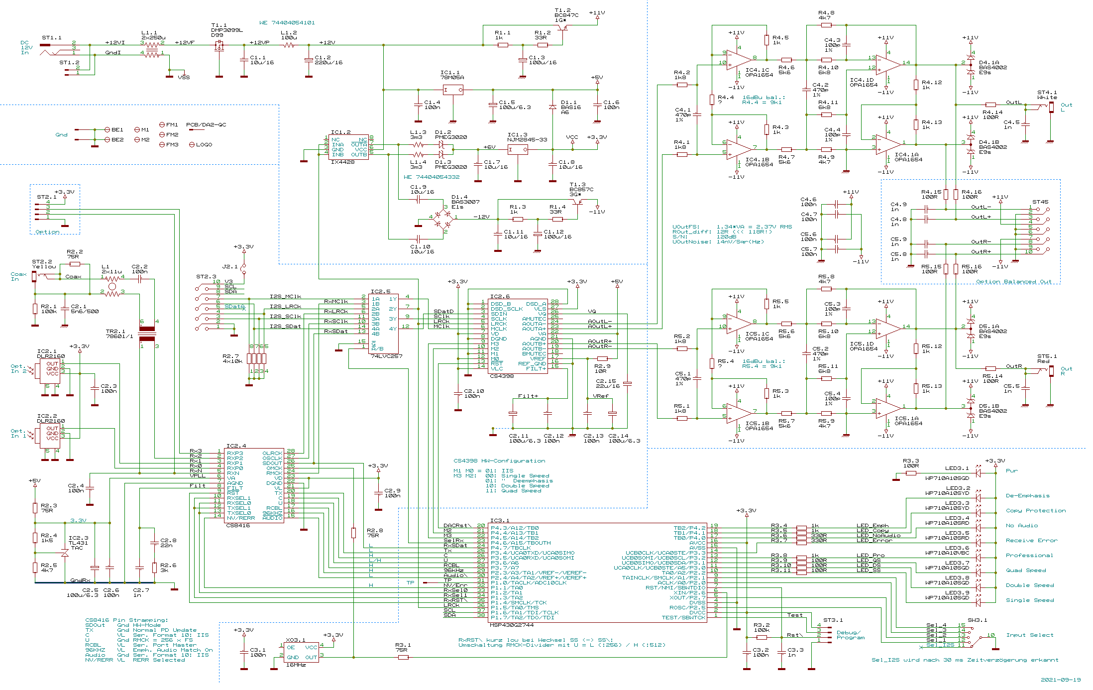
The DAC DA2-QC
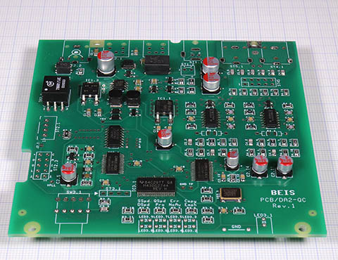

Pictures: View of the SMD-only DAC and the DAC completed with THT components, without additional connections.
 This circuit does not contain any unusual tricks either.
What I wrote for the circuit of the ADC also applies to the generation of the operating voltage. The operating current is always less than 130 mA for the current prototype.
Additional external balanced outputs, e.g. XLR sockets, can be connected directly via a pin header. The output levels (normally 2 Vrms or 4 Vrms at the balanced outputs) can be increased if additional THT resistors are inserted at the places kept free for this purpose.
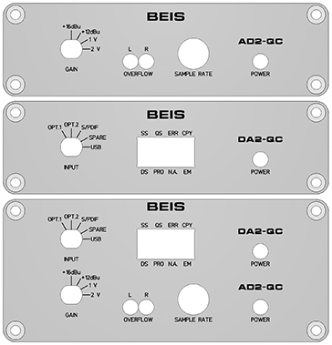
8 LEDs are used for indication as with the DA24QS:
- Sample Rate: Single-, Double- or Quad-Speed
- Professional Format (AES3)
- The audio signal is faulty (Error)
- The signal present is not an audio signal
- The Copy bit
- The Preemphasis signal
Of course, the DAC cannot be externally synchronized. Instead, there is a 10-pin I2S connector through which it can receive an external I2S signal. This is intended for the bidirectional USB interface UIC22. Accordingly, the input selector switch has 5 positions:
- #1 and #2 for the two on-board Toslink inputs,
- #3 for the on-board S/PDIF input,
- #4 for an external signal, e.g. AES3 or another S/PDIF input and
- #5 for the I2S input.
An external AES3 or S/PDIF input requires at least one transformer and resistor externally in addition to the jack. For an S/PDIF input, further ESD and EMC measures are recommended, as can also be seen in the circuit diagram for input #3.
Word Clock Synchronization with the AD2-XS

The AD2-XS
Again and again I am asked for Word Clock synchronization, again and again I had to cancel. Until now.
The story of a late VCXO success
This module is rather extraordinary. A circuit, with which ADCs can be synchronized by a word clock signal, is in principle simple: Take a PLL IC, in the simplest case e.g. a 'HC4046 with the required external circuitry, add a divider chain with another IC, e.g. 'HC4040, and you're done. But: No, that simple and primitive is out of the question in practice.
First, the RC oscillator of such a PLL IC shows a much higher jitter than a crystal oscillator (XO). And an XO is already a common standard for a high quality audio ADC. An RC oscillator is out of the question, at least for me.
Secondly, it is not possible to cover a wide range of sample rates, because the ADC ICs and possibly also the serial Tx ICs need, depending on the sample rate, information whether it is single, double or quad speed and also differently divided oscillator frequencies and additional control signals.
 While the second aspect is still comparatively easy to solve, the first was an unsolved problem for me for many years. A PLL with a crystal oscillator needs a voltage controllable crystal oscillator, a VCXO. The frequency of such a VCXO can be changed (also called "pulled") only in a relatively small range. Often this is no more than other normal XOs offer as basic accuracy and much less than you need to cover even the nominal deviations of your own VCXO.
VCXOs for the two required frequencies are already exotic, and if you then add requirements for two from the same series for the correct operating voltage, a suitable design, etc., you can no longer expect them to be available for unusually high pulling ranges. The chances of success for a solution with VCXOs, which can be bought in small quantities from stock, are so low that I have given up this way because of that.
It was many years ago that I once got a sample production especially according to my wishes. The pulling range of 100 ppm together with the basic accuracy was just sufficiently high. With this I developed the XS-AD24. Only: To produce a small number of pieces, I would have had to buy 2 x 1000 VCXOs. I am not a professional big company with large quantities, so this was far above my pain threshold. On top of that, I was later informed that the pulling range of the samples in the series would no longer be fully complied with, and even later that it was no longer possible to manufacture these VCXOs at all.
Recently, I returned to the subject. Many attempts with different concepts, crystals, oscillator circuits and ICs and varicaps failed. And in the end, success came: A VCXO, which can be pulled in a range of more than 400 ppm (± 200 ppm), and can also be switched between 2 frequencies or crystals. 3.3 V operating voltage, components from the catalog - eureka! With this concept, the desired word clock VCXO synchronization could finally be realized.
The AD2-XS
Picture: The AD2-XS is connected to the AD2-QC via a short ribbon cable.
The AD2-XS is connected to the AD2-QC via a 10-pin ribbon cable. Several AD2-QC can be controlled by one AD2-XS at the same time, but at some point it might be necessary to connect a line driver to the AD2-XS for this purpose. It is simply looped into the flat cable. Prepared for this is the above mentioned small module called I2S-Buf.
The AD2-XS is supplied with operating voltage (3.3 V) from the AD2-QC. The operating current from the AD2-QS with the AD2-XS connected is always less than 140 mA in the current prototype.
The AD2-QC recognizes the AD2-XS and disables its own clock generation and local sample rate setting. On the AD2-XS, 2 buttons can be used to select 12 different sample rates at which the ADC should operate when no word clock signal is present at any of the 12 frequencies within the valid range. These frequencies are indicated by 12 yellow LEDs. Valid are these 12 sample rates in a range of about ± 150 ppm of the nominal frequency. They are indicated with a green LED "EXT", and in this operating case the yellow LEDs also indicate the actual sample rate. Invalid word clock signals are indicated by a red LED "ERR".
The phase comparator is the PC2 of a 74HCT9046. I have to say that other phase comparators, especially those of the 4046 PLL circuits or e.g. the 74HCT7046 show an unacceptable behavior for such a purpose. Also many other phase comparators seem to me to show this behavior. I described this in the article "4046 vs. 9046". Unfortunately the 74HCT9064 is not produced any more, therefore I have (hopefully) enough of it "bunkered" for the time being.
For the word clock input signal there are the usual BNC sockets. One is the input socket, a second would be the output for a looped through signal. A toggle switch is used to terminate the input with 75 Ω or switch it to the output jack without termination.
Of course, the whole thing is also controlled by a µC that measures the frequency of the external sample rate and decides if it can be synchronized, drives the LED indicators accordingly, selects the divider factors for I2S signals needed for the ADC, and of course displays and stores the manual frequency selection.
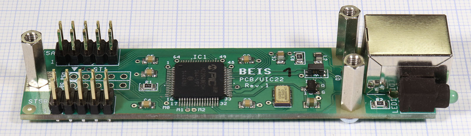
The USB interface UIC22

I already wrote elsewhere about the DA2USB, why and with how much effort the DA2USB was developed. Carsten, who is responsible for this software stroke of genius, is currently working on an extension that will enable the firmware of the unidirectional DA2USB for bidirectional operation, i.e. ADC → USB and USB → DAC. This is not a simple extension, this is actually a completely new software architecture. The hardware, on the other hand, is trivial. The point of the development is also to create a small plug-on module for the AD2-QC, to which a DA2-QC can also be connected and operated for simultaneous input and output of audio signals.
Pictures: The UIC22 can be connected via a ribbon cable as well as plugged on directly.
Attention: The UIC22 does not contain its own audio clock generator. It cannot operate a DAC without an ADC connected at the same time! In principle it would be possible to operate it with an external I2S generator, e.g. the AD2-XS, but would that make sense? Probably not. In contrast to pure USB ADCs, there are so many USB DACs available that it would make little sense to try to compete with them with such a solution.
The UIC22 can only transmit the two audio channels (left and right) of an ADC and a DAC. Signals from multiple ADCs or DACs cannot be transmitted.
The UIC22 behaves like a DA2USB, i.e. it logs on to the PC as a USB Audio Class 2 device with the applied sample rate in its name and is immediately ready for operation without any further driver installation or the like.
Enclosures
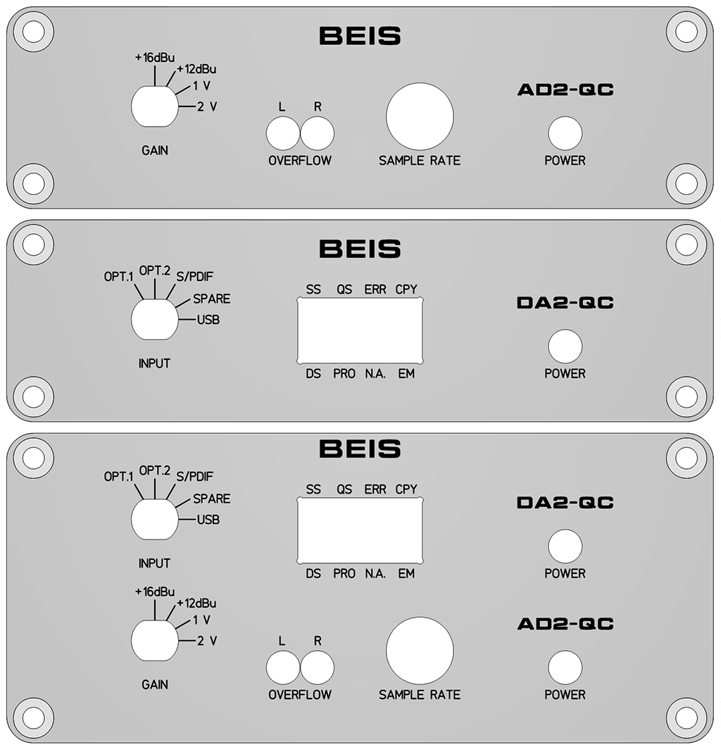
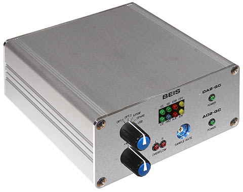
I would also like to provide complete enclosures with front and rear panels for the converters in this project, instead of enclosures with unfinished front and rear panels, as I have done with the previous ADCs un DACs. However, I don't expect large quantities, and because manufacturing decent front panels in small quantities is expensive, I can only limit myself to very few variations of the many possible combinations and options, if at all. At least one enclosure for the basic AD2-QC (with USB interface) and one for the DA2-QC should be available. Both would be 105 mm wide, 104 mm deep and 30 mm high. The kits are intended for use with 100 mm long continuous cast aluminum enclosures of the AKG 105... series from Fischer Elektronik GmbH & Co. KG. For larger housings, e.g. for AD2-QC + AD2-XS + 3 x XLR, the 165 mm wide AKG 165... series could also be considered.
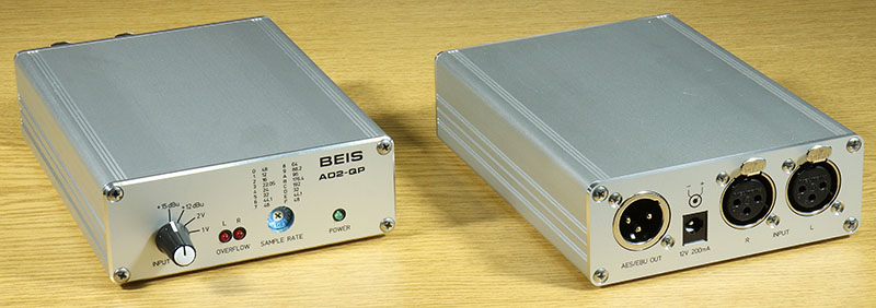
So far I have not had any front or rear panels made. But I made a photo montage, which shows how a complete enclosure for an ADC together with a DAC could look like. This enclosure would have a height of 46 mm:
Also, I would like to prepare and provide a number of design files for front and rear panels of different variants of ADCs, DACs, additional modules, XLR connectors, etc.. These design files can then be comfortably modified and produced with the intuitive "Front Panel Designer" from Schaeffer AG (http://www.schaeffer-ag.de, international: Front Panel Express, http://www.frontpanelexpress.com). However, as mentioned, this is not cheap.
Epilogue
As mentioned, I would like to offer these kits, but my hands are tied indefinitely. Probably there will be additional modules, such as boards for analog and digital outputs or a microphone or phono preamplifier. With the relatively small quantities I expect, this is difficult to organize easily or even economically. The future will show what works and what doesn't.
Epilogue to the epilogue:
Yes, it's nice to see that at least the ADC kits are now available after all. But for all the other fine projects, I still have my doubts.
| Last update: September 25th, 2025 |
Questions? Suggestions? Mail
Me! |
Uwe Beis |